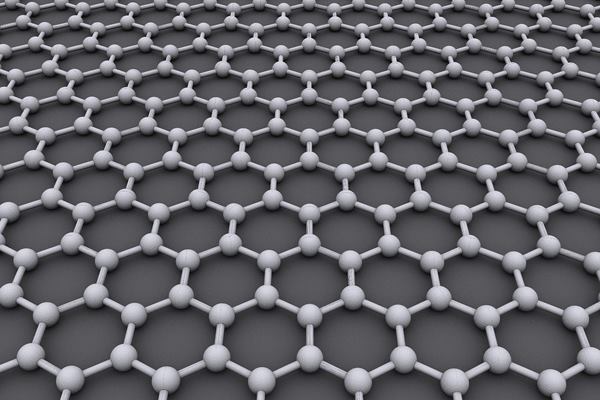
Graphene is the nanomaterial of the moment. It’s the strongest, thinnest, stiffest, and most conductive substance known to date, and it derives from a ubiquitous source: graphite (think pencil lead). In 2004, two scientists from the University of Manchester in the U.K. found a way to isolate graphene, which is a single layer of carbon atoms arranged in a hexagonal lattice. The secret? Sticking tape on a graphite crystal, transferring it to a substrate, and replicating the process on each subsequent substrate. The work won them the 2010 Nobel Prize in physics, and graphene the spotlight. Now, researchers are exploring uses for the material that range from solar panels to structural members.
Once merely a “laboratory curiosity,” graphene may soon be a common engineering material, says Jeffrey Kysar, a mechanical engineering professor at Columbia University who researches ways to measure and improve the strength of graphene.
Mechanical exfoliation, the process used by the Nobel laureates who peeled one-atom-thick layers off of graphite, is time-consuming and doesn’t yield much. Chemical vapor deposition is more efficient but brings its own challenges. Metallic foil is saturated with carbon, which diffuses as it cools and assembles into one or more layers of graphene. But the strong chemicals, or etchants, used to separate the graphene and foil weaken the already unstable bonds between graphene’s flakes.
Kysar compares the graphene’s arrangement to ice crystals on the exterior of a cold car window. “Small patches of graphene are connected or zipped together, [creating] an imperfect region of the atomic lattice,” he says.
In a study published in Science last year, Kysar’s team found that using weaker etchants kept the bonds intact and resulted in larger graphene sheets that are only slightly weaker (approximately 10 percent) than the highly desired crystalline version. Though “large,” here, is measured in millimeters, Kysar says, the process is scalable.
Researchers at Northwestern University are also scaling up graphene collection. Detailed in a 2013 report in The Journal of Physical Chemistry Letters, their graphene-based ink can print highly conductive and bendable electrode patterns that could power next-generation flexible electronics or other media displays. Mark Hersam, director of Northwestern’s Materials Research Science and Engineering Center, says his lab and the university are in talks with potential partners to supply ink to the industry.
“The growing misconception is that graphene has already reached its potential,” Hersam says. “A lot of the fundamental experiments have been done, but [there’s] a big difference between a research lab and finding the market need for such a material.”
Slowly, but surely, graphene is making its way from the lab to the market. Spanish nanotech research and manufacturing group Graphenano is marketing its graphene- and limestone-based paint (left) as ultra-strong and eco-friendly. Sports-equipment maker Head is reinforcing the shaft of its tennis racquets with graphene to increase their resilience while redistributing the weight to the head and handle to give players more power and control. Meanwhile, researchers in Spain and the U.K. found that adding highly conductive graphene in some solar cells can lower fabrication temperatures, cut production costs, and lead to more affordable photovoltaics. And from the Nobel Prize–winners comes the subsequent discovery that graphene-oxide sheets stacked in a mesh-like lattice are permeable only to water molecules, adding reverse-osmosis water filtration to the list of the material’s potential uses.
Structural applications are also on deck. Kysar is one of several researchers trying to engineer graphene composites to handle tensile loads. “The first step is to make relatively small pieces of this composite material and … [then] we’ll figure out how to make the big pieces out of it,” he says. “So start small and get bigger.”
Spanning a 3D space with a 2D material will be a feat, but graphene has already proven capable of taking on more than its own weight.
Take a tour of a material synthesis laboratory at Columbia University where the Science paper’s co-author Dr. James Hone grows graphene: